
Thank you for writing to us. One of our executive will reach back to you through your submitted medium. In case there’s an urgency, feel free to connect over WhatsApp for faster response.
Prefer calling? Dial +9108042755673 (International callers) or 08042755673 (Indian callers).
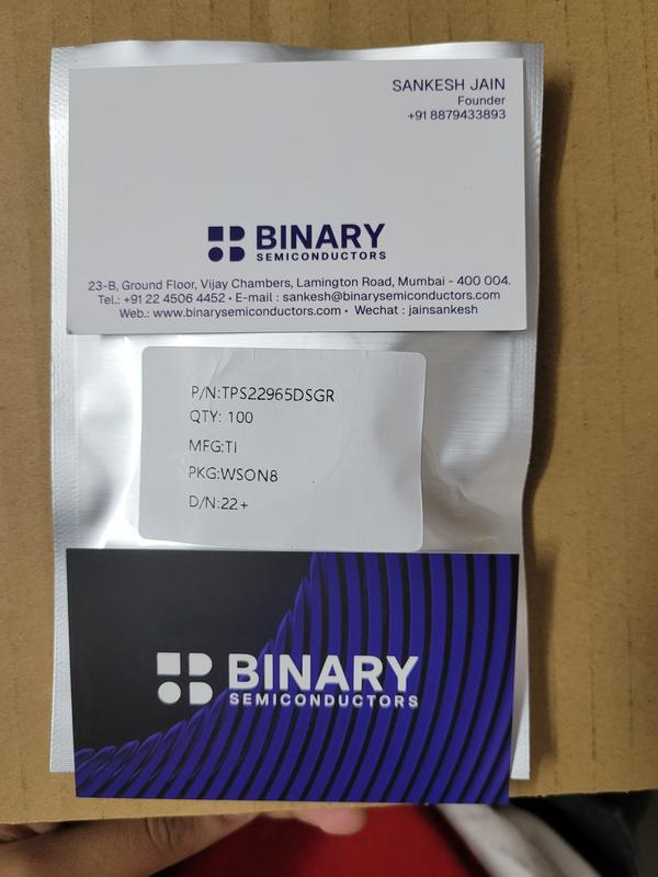
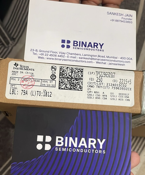
The TPS22965x is a single channel load switch that
provides configurable rise time to minimize inrush
current. The device contains an N-channel MOSFET
that can operate over an input voltage range of 0.8 V
to 5.7 V and can support a maximum continuous
current of 6 A. The switch is controlled by an on and
off input (ON), which is capable of interfacing directly
with low-voltage control signals. In the TPS22965, a
225-Ω on-chip load resistor is added for quick output
discharge when switch is turned off.
The TPS22965x is available in a small, space-saving
2-mm × 2-mm 8-pin SON package (DSG) with
integrated thermal pad allowing for high power
dissipation. The device is characterized for operation
over the free-air temperature range of –40°C to
+105°C.
The TPS22965x is a single channel load switch that
provides configurable rise time to minimize inrush
current. The device contains an N-channel MOSFET
that can operate over an input voltage range of 0.8 V
to 5.7 V and can support a maximum continuous
current of 6 A. The switch is controlled by an on and
off input (ON), which is capable of interfacing directly
with low-voltage control signals. In the TPS22965, a
225-Ω on-chip load resistor is added for quick output
discharge when switch is turned off.
The TPS22965x is available in a small, space-saving
2-mm × 2-mm 8-pin SON package (DSG) with
integrated thermal pad allowing for high power
dissipation. The device is characterized for operation
over the free-air temperature range of –40°C to
+105°C.
The STMPS2141, STMPS2151, STMPS2161, STMPS2171 power distribution switches are intended for applications where heavy capacitive
loads and short-circuits are likely to be encountered. These devices incorporate 90 mW N-channel MOSFET high-side power switches for
power distribution. These switches are controlled by a logic enable input.
When the output load exceeds the current limit threshold or a short is present, the device limits the output current to a safe level by switching into a constant current mode. When continuous heavy overloads and short-circuits increase the power dissipation in the switch, causing the junction temperature to rise, a thermal protection circuit shuts the switch off to prevent damage. Recovery from a thermal shutdown is automatic once the device has cooled sufficiently. Internal circuitry ensures the switch remains off until a valid input
voltage is present.
The UCC27282 is a robust N-channel MOSFET driver with a maximum switch node (HS) voltage rating of 100 V. It allows for two N-channel MOSFETs to be controlled in half-bridge or synchronous buck configuration based topologies. Its 3-A peak source and sink current along with low pull-up and pull-down resistance allows the UCC27282 to drive large power MOSFETs with minimum switching losses during the transition of the MOSFET Miller plateau.
Since the inputs are independent of the supply voltage, UCC27282 can be used in conjunction with both analog and digital controllers.
The input pins as well as the HS pin are able to tolerate significant negative voltage, which improves system robustness. Input interlock further improves robustness and system reliability in high noise applications. The enable and disable functionality provides additional system flexibility by reducing power consumption by the driver and responds to fault events within the system. 5-V UVLO allows systems to operate at lower bias voltages, which is necessary in many high frequency applications and improves system efficiency in certain operating
modes.
Small propagation delay and delay matching specifications minimize the dead-time requirement which further improves efficiency.
Under voltage lockout (UVLO) is provided for both the high-side and low-side driver stages forcing the outputs low if the VDD voltage is below the specified threshold. An integrated bootstrap diode eliminates the need for an external discrete diode in many
applications, which saves board space and reduces system cost. UCC27282 is offered in a small package enabling high density designs.
INTEGRATED CIRCUITS
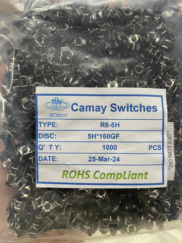
Still searching for 6mm push button tactile switch?
Vijay Chambers, 23-B, Tribhuvan Rd, opp. Dreamland Cinema, Grant Road East, Shapur Baug, Grant Road